
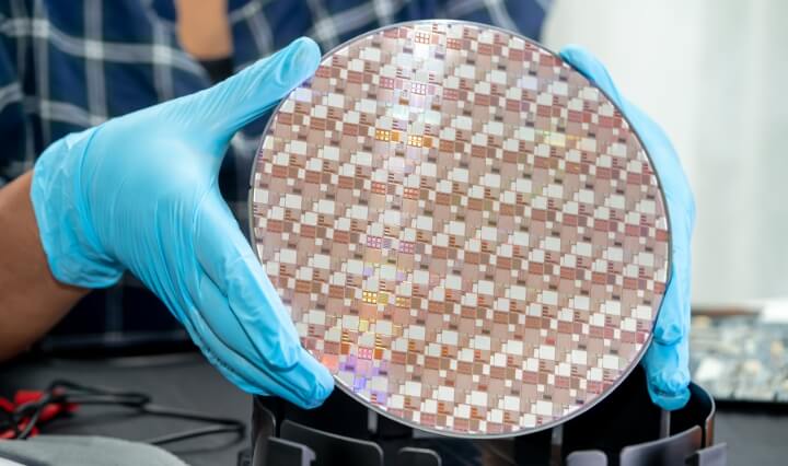
ASIC Physical Design
ChipNova provides comprehensive ASIC Physical Design services for semiconductor companies developing high-performance and reliable integrated circuits. Our expertise spans floorplanning, placement, clock tree synthesis, routing, and signoff implementation.
From netlist handoff and design planning to timing closure and physical verification, we deliver optimized implementations that meet power, performance, area, and manufacturing requirements.
Engineering Capabilities
- Advanced Floorplanning & Design Partitioning
- High-Performance Placement & CTS Optimization
- Optimized Routing For Timing And Congestion
- Comprehensive STA, DRC & LVS Signoff Flow
- Production-Ready GDSII Delivery Solutions
End-to-End Physical Design Services
Our engineering team executes complete ASIC implementation flows including floorplanning, placement, clock tree synthesis, routing, timing analysis, and physical signoff for advanced technologies.
We focus on delivering high-quality designs with optimized timing, power, area, and reliability characteristics while ensuring smooth integration into complex SoC development programs.
Delivering Manufacturing-Ready Designs
Our ASIC Physical Design services help clients accelerate chip development while maintaining quality, accuracy, and implementation efficiency across advanced semiconductor technology nodes.
With strong expertise in implementation, timing closure, and signoff verification, ChipNova delivers reliable solutions ready for successful tapeout and silicon realization.
